Ecer asks for your consent to use your personal data to:
Personalised advertising and content, advertising and content measurement, audience research and services development
Store and/or access information on a device
Your personal data will be processed and information from your device (cookies, unique identifiers, and other device data) may be stored by, accessed by and shared with 135 TCF vendor(s) and 65 ad partner(s), or used specifically by this site or app.
Some vendors may process your personal data on the basis of legitimate interest, which you can object to by do not consent. Contact our platform customer service, you can also withdraw your consent.
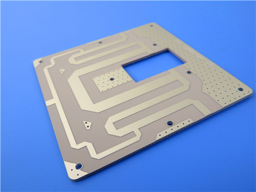
{"title":"4-Layer Rogers RO3210 High Frequency PCB 1.22mm with ISIG Finish","imgUrl":"https:\/\/img.chinax.com\/nimg\/53\/50\/7bfdcd4d13526bd4b02c12c41935-200x200-1\/4_layer_rogers_ro3210_high_frequency_pcb_1_22mm_with_isig_finish.jpg","attrs":{"Copper weight":"1oz outer layer \/ 1oz inner layer","Base material":"RO3210 + RO4450F PP","Silkscreen":"No","Surface finish":"Silver plating + Gold plating"}}
{"title":"RO3003 + Tg170 FR-4 Hybrid 4-Layer PCB Ceramic-Filled PTFE High Frequency Circuit Board","imgUrl":"https:\/\/img.chinax.com\/nimg\/f3\/d3\/872ff7e16d9c24a99f01053b7652-200x200-1\/ro3003_2b_tg170_fr_4_hybrid_4_layer_pcb_ceramic_filled_ptfe_high_frequency_circuit_board.jpg","attrs":{"Layer count":"4 layers","Solder mask":"Green","Brand Name":"Bicheng","Model Number":"BIC-289.V1.0"}}
{"title":"Blind Via PCB Built on Tg150\u2103 FR-4 With Immersion Gold 4-Layer FR-4 Circuit Board","imgUrl":"https:\/\/img.chinax.com\/nimg\/8e\/e4\/3932321441a8351e28fc058d939c-200x200-1\/blind_via_pcb_built_on_tg150_e2_84_83_fr_4_with_immersion_gold_4_layer_fr_4_circuit_board.jpg","attrs":{"Brand Name":"Bicheng","Model Number":"BIC-452.V1.0","Certification":"UL, ISO9001, IATF16949","Place of Origin":"CHINA"}}
{"title":"6-Layer Hybrid PCB 10 mil with Blind Via","imgUrl":"https:\/\/img.chinax.com\/nimg\/58\/e2\/91b96e4d0b08bae4469126ee55f1-200x200-1\/6_layer_hybrid_pcb_10_mil_with_blind_via.jpg","attrs":{"Brand Name":"Bicheng","Model Number":"BIC-081.V1.0","Certification":"UL, ISO9001, IATF16949","Place of Origin":"CHINA"}}
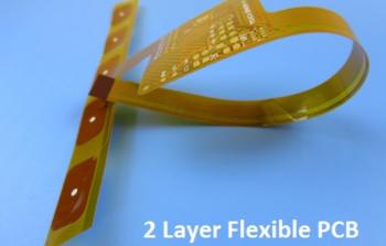
{"title":"Flexible Printed Circuit (FPC) Built on 2oz Polyimide With Immersion Gold and Yellow Coverlay for Interface Module","imgUrl":"https:\/\/img.chinax.com\/nimg\/3b\/38\/46729d68f141dade767785362307-200x200-1\/flexible_printed_circuit_28fpc_29_built_on_2oz_polyimide_with_immersion_gold_and_yellow_coverlay_for_interface_module.jpg","attrs":{"Brand Name":"Bicheng","Model Number":"BIC-313.V1.0","Certification":"UL, ISO9001, IATF16949","Place of Origin":"CHINA"}}
Founded in 2003, Bicheng Electronics Technology Co., Ltd. is a well-established supplier and exporter of high-frequency PCBs based in Shenzhen, China. With 23 years of industry experience, the company serves global sectors such as cellular base station antennas, satellite communications, high-frequency passive components, microstrip and stripline circuits, millimeter-wave equipment, radar systems, and digital RF antennas. Bicheng's high-frequency PCBs are primarily manufactured using three major high-frequency material brands—Rogers Corporation, Taconic, and Wangling—with dielectric constants ranging from 2.2 to 10.2. Headquartered in the economically vibrant city of Shenzhen, Bicheng PCB operates with a philosophy centered on serving small and medium-sized enterprises, offering a wide variety of circuit boards to meet diverse market demands.
Main Business & PCB Applications
The company upholds the highest manufacturing standards to deliver products known for exceptional quality, performance, and reliability. In addition to high-frequency PCBs, Bicheng has divisions specializing in FR-4 circuit boards, high frequency PCBs, and RF PCBs, supporting everything from prototyping and small-batch production to mass manufacturing. The company actively develops value-added PCB solutions, including HDI, quick-turn production, impedance control, heavy copper, and backplane boards. This strategic focus enables Bicheng to offer an extended and complementary product range, forming an integrated line that spans from low-end to high-end PCBs. These circuit boards are widely used in home appliances, portable and consumer electronics, medical devices, aerospace, and telecommunications.
We are a service-oriented company specializing in PCB fabrication and PCBA delivery. Our core team has over 20 years of industry experience, with in-depth knowledge of manufacturing processes for multi-layer PCBs, HDI boards, rigid-flex boards, high-frequency and high-speed boards.
We do not provide PCB design services. Our expertise lies in efficiently and reliably transforming customer-provided design files (Gerber, BOM, pick-and-place files, etc.) into manufacturable, high-quality products.
Our Services
OEM Manufacturing
With complete design files provided by customers, we manage the entire PCB fabrication and PCBA process:
DFM Review: Engineering validation of Gerber files before production—checking trace width and spacing, hole sizes, stack-up structure, impedance control, and other critical parameters to identify and resolve manufacturing risks early.
Production Resource Matching: Optimal production line allocation based on layer count, material type (FR4, high-frequency materials, metal-core, etc.), surface finish requirements (ENIG, OSP, HASL, etc.), and delivery schedule.
End-to-End Quality Control: Full-process monitoring from material cutting, lamination, drilling, and plating to solder mask, surface finishing, profiling, and electrical testing. Mandatory inspection hold points at critical stages, with 100% electrical testing on finished boards.
Leveraging long-established supply chain partnerships, we offer:
Component Sourcing: BOM kitting services through reliable component channels, reducing customers' administrative costs of fragmented procurement.
Flexible Capacity Coordination: Agile capacity deployment across multiple manufacturing partners based on order volume, process complexity, and delivery urgency to ensure on-time delivery.
Cost Optimization Recommendations: Reference suggestions on material alternatives, panelization optimization, and surface finish selection to reduce costs without altering the original design.
Quality System
All manufacturing partners are certified with:
ISO 9001 Quality Management System
IATF 16949 Automotive Quality Management
ISO 13485 Medical Devices Quality Management
UL Safety Certification
All products are RoHS and REACH compliant.
Each shipment includes a complete inspection report (impedance test, solderability test, cross-section analysis, etc.) with full traceability.
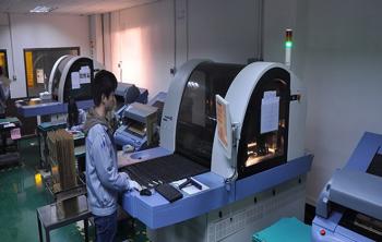
PCB Pattern Plating
PCB Washing
Developing
Production Line:
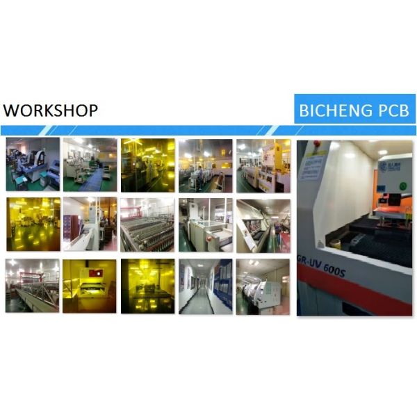
Bicheng Electronics operates two major production bases, strategically located in Shenzhen and Jiangmen.
The Shenzhen factory employs over 300 staff and has a monthly output exceeding 10,000 square meters of PCBs. As a brand-new facility, it specializes in quick-turn prototypes and small-volume production.
The Jiangmen factory features two new industrial buildings spanning approximately 15,000 square meters, specifically designed for mass production. Equipped with state-of-the-art automated machinery sourced from Israel, Japan, Germany, and Taiwan, the Jiangmen facility produces up to 30,000 square meters per month for 2- to 10-layer PCBs. The establishment of this plant has significantly strengthened Bicheng’s capacity to supply high-end PCBs to both domestic and global markets.
With a strong and diverse product portfolio, Bicheng serves customers worldwide. Our offerings include multi-layer boards (up to 32 layers), flex-rigid combinations, heavy copper PCBs, high-frequency and high-speed boards, and HDI, among other types.
We are committed to becoming a leading diversified PCB supplier known for precision-engineered products. Our mission is to create lasting value for our customers while building a promising future for our employees.
R&D:
Design For Manufacture
Serial NO.
Procedure
Item
Manufacturing capability
Large volume (S<100 m²)
Middle volume (S<10 m²)
Prototype(S<1m²)
1
Inner layer (18um, 35um, 70um etc are finished copper. If not mentioned copper, finished 1oz is the default value )
Min. distance from board edge to conductor(no copper exposured)(inner layer)
14 mil(35um)
12 mil(35um))
8 mil(35um)
12
Maximum copper weight(Inner layer and outer layer)
3 OZ( 105 um )
4 OZ ( 140 um )
6 OZ( 210 um )
13
Core with different copper foil on both sides
/
18/35,35/70 um
18/35,35/70 um
14
Laminating
Tolerance of laminate thickness
±10% PCB thick
±10% PCB thick
±8% PCB thick
15
Maximum laminate thickness
4.0mm
6.0mm
7.0mm
16
Laminate alignment accuracy
≤±5 mil
≤±4 mil
≤±4 mil
17
Drill (18um, 35um, 70um etc are finished copper. If not mentioned copper, finished 1oz is the default value )
Min.drill bit diameter
0.2 mm
0.2 mm
0.2 mm
18
Min.slot router diameter
0.60 mm
0.60 mm
0.60 mm
19
Min.tolerance of PTH slots
±0.15mm
±0.15mm
±0.1mm
20
Max.aspect ratio
1:08
1:12
1:12
21
Hole tolerance
±3mil
±3mil
±3mil
22
Space of via to via
6mil(same net),12mil(different net)
6mil(same net),14mil(different net)
4mil(same net),12mil(different net)
23
Space of component hole to component hole
12mil(same net),16mil(different net)
12mil(same net),16mil(different net)
10mil(same net),14mil(different net)
24
Etching
Min.width of etching logo
10mil(18um),12 mil (35um),12 mil(70um)
8mil(18um),10mil(35um),12 mil(70um)
6mil(18um),8 mil(35um),12mil(70um)
25
Etch factor
1.6-2.2
1.6-2.2
1.6-2.2
26
Outer layer(18um, 35um, 70um etc are finished copper. If not mentioned copper, finished 1oz is the default value )
Min.via pad diameter
20mil
16mil
16mil
27
Min.BGA pad diameter
12mil
12mil
10mil
28
Min.track and spacing
5/5mil(18um)
4/4mil(18um)
3/3.5mil(18um)
5/5mil(35um)
4/4mil(35um)
3/4mil(35um)
7/9mil(70um)
6/8mil(70um)
6/7mil(70um)
9/11mil(105um)
8/10mil(105um)
8/9mil(105um)
13/13mil(140um)
12/12mil(140um)
12/11mil(140um)
29
Minimum grid
10/10mil(35um)
8/8mil(35um)
4/8mil(35um)
30
Min.space (conductor to pad, pad to pad)
6mil(18um)
5mil(18um)
4mil(18um)
6mil(35um)
5mil(35um)
4mil(35um)
9mil(70um)
8mil(70um)
7mil(70um)
11mil(105um)
10mil(105um)
9mil(105um)
13mil(140um)
12mil(140um)
11mil(140um)
31
Solder mask (18um, 35um, 70um etc are finished copper. If not mentioned copper, finished 1oz is the default value )
Maximum via-plug diameter
0.5mm
0.5mm
0.5mm
32
Min.width of solder mask bridge
Green:5mil(35um)
Green:4mil(35um)
Green:4mil(35um)
33
Yellow:5mil(35um)
Yellow:4mil(35um)
Yellow:4mil(35um)
34
Blue:5mil(35um)
Blue:4mil(35um)
Blue:4mil(35um)
35
Black:6mil(35um)
Black:6mil(35um)
Black:6mil(35um)
36
White:6mil(35um)
White:6mil(35um)
White:6mil(35um)
37
All of Matt:6mil
All of Matt:6mil
All of Matt:6mil
38
Green:5mil(70um)
Green:4mil(70um)
Green:4mil(70um)
39
Yellow:5mil(70um)
Yellow:4mil(70um)
Yellow:4mil(70um)
40
Blue:5mil(70um)
Blue:4mil(70um)
Blue:4mil(70um)
41
Black:6mil(70um)
Black:6mil(70um)
Black:6mil(70um)
42
White:6mil(70um)
White:6mil(70um)
White:6mil(70um)
43
Open solder mask
4mil(35um)
4mil(35um)
3mil(35um)
44
Solder mask coverage
4mil(35um)
4mil(35um)
3mil(35um)
45
Min.width of solder mask text
9mil(35um)
9mil(35um)
8mil(35um)
46
Min.thickness of Solder mask
9um(35um)
9um(35um)
9um(35um)
47
Max.thickness of solder mask
30um(35um)
30um(35um)
30um(35um)
48
Silkscreen
Min.width of silkscreen text
6mil
6mil
5mil
49
Min.height of silkscreen text
35mil
35mil
30mil
50
Min.space from silkscreen to pads
6mil
6mil
5mil
51
Colour of silkscreen
White, Black, Yellow
52
Carbon ink
Carbon ink covers conductor or pads
14mil
13mil
12mil
53
Mid distance from carbon ink to pads
12mil
11mil
Our Team:
Every day, we strive to improve, keep progressing, and never stand still. We believe that teamwork is the key to success, and our commitment to the creative process only makes us stronger.
Guided by modern scientific management and real-time information sharing through network technology, we have created a highly efficient working environment. Our skilled manufacturing expertise helps equipment achieve its best performance. With our high-quality PCBs and flexible cooperation, you will experience professional, value-added service.
At Bicheng, your specific needs are met, while our success is driven by innovative products and a competitive edge.
History:
BichengPCB is the brand of Shenzhen Bicheng Electronics Technology Co., Ltd. Its origins date back to 2003, when it was known as Bicheng Enterprise Company, specializing in blank printed circuit boards for single-sided and double-sided PCBs.
To meet growing market demand, the company began offering multilayer PCBs in 2008, with layer counts reaching up to 32 layers. In 2010, Bicheng introduced high-frequency materials for applications involving antennas, amplifiers, and radio products.
As the company evolved, metal-core PCBs and hybrid PCBs were successfully trialed and received high praise. In 2014, the company underwent restructuring and reform, with Bicheng taking on a new role within the organization—focusing on global market sales and after-sales services.
By 2020, Bicheng had completed a full range of integrated PCB products, including high-frequency/microwave PCBs, multi-layer/hybrid PCBs, metal-core PCBs, and flexible circuits.
Today, Bicheng’s products can be found in over 100 countries and regions around the world.